vrijdag 6 december 2019

Differentiating real signals from spurs in the tiny spectrum analyzer

When measuring the harmonics from my Softrock Ensemble RXTX I noticed a number of strange (e.g. non harmonic) signals such as at 0.8MHz , 9MHz, 12.8MHz and 13.8MHz
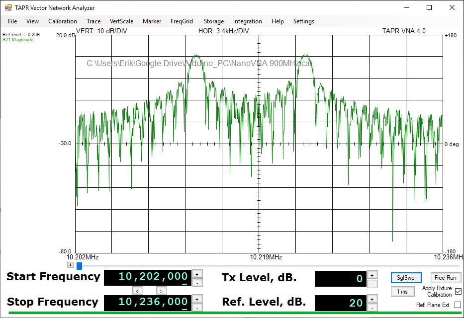
Is the output of the RXTX really that bad, or are these spurs and mirrors? Below is a 4 times averaged scan of the output of the TXRX through a 60dB attenuator with RBW set to automatic


When wobbling the first IF around 433MHz, real input signals should stay at the same frequencies but mirrors or internally generated spurs may change to different frequencies or disappear altogether.
This is possible because  the 434MHz IF filter is about 1MHz wide , much wider than the currently selected RBW bandwidth of about 20kHz.
Luckily I implemented this wobbling for the 2GHz spectrum analyzer and I could enable it by switching on "Spur Reduction"
Combined with 4 times averaging this positions the 434MHz IF at 4 different frequencies, still within its 1MHz bandwidth but twice the RBW apart and the averaging should reduce the signals that change position in the scan.
The impact is easily seen as most spurs and mirrors almost disappear giving confidence the RXTX is not that bad.


There is some different in the amplitude of the real signals at 7.11MHz and 14.22MHz as the IF filter at 434MHz is not really a flat top filter and the calculated IMD changes a bit but the difference (about 1dB) is acceptable
The SW spur reduction nicely compensates for the absence of good HW filtering and helps to keep the tiny spectrum analyzer small and easy to build.

maandag 2 december 2019

Further tuning of the 2GHz cavity filter

Some more tuning resulted in a nice flat top of the pass band


At least flat within 0.5dB
Center frequency at 2020.7MHz, 
S21 -5.1dB
-3 dB width 3.3MHz
-40dB width 14MHz

Tiny home build spectrum analyzer

Building and tuning GHz cavities is not everyone's hobby but if you need a zero till a couple of hundred MHz spectrum analyzer there is a much simpler build possible.


This is all you need to measure signals between  0 and 400MHz at levels between -80dbm and -20dBm
Top blue module is a mixer. Can be found on eBay either as complete module (ADE-1) for 10$ of you only buy the mixer (AD-25MH (much better level 13 mixer), 5pc for 4$) and put it on a small PCB
The two small identical blue modules are SI4432 modules (do NOT use SI4463 modules as these use non overlapping bands) that can be found on eBay for less than 2$
The one directly connected to the mixer acts as a tunable LO with 20dBM  output between 433MHz and 860MHz
The copper module is a 433MHz band pass filter you either buy from eBay for 25$ or build yourself from two EPCOS SAW filters and two SMD inductors for less then 10$
Datasheet here
The bottom blue module is the receiver SI4432. Its set at a fixed frequency of 433MHz and does the the logarithmic signal strength measurement. The officiel range is -120dB till 0dB but the range is limited in practise between -100dBm and -20dBm as above -20dBm the SI4432 will start to produce all kind of intermodulation products. 
The module with the USB plug is an Arduino zero compatible to provide the 3.3Volt and to control the SI4432 modules (these need 3.3V MISO/MOSI/CLK)

Some real measurements
Scan from 0 to 5MHz


The phase noise of the LO SI4432 is very visible but the 3kHz RBW results in a nice sharp peak. The noise floor is not very flat but no spurs
The AD9851 clearly delivers a nice clean signal at 1MHz through 40dB of attenuators

Switching to 0-100MHz you get


RBW now set to 300kHz. Output of the same AD9851 at 46MHz
Some small spurs but contrary to cheap "spectrum analyzers" you can buy on eBay which are basically nothing more than a LO, a mixer to DC, a LF RBW filter and a log detector, this SA does not have the many spurs from the harmonic modes of the LO due to proper filtering. The second harmonic from the AD9851 at 92MHz is clearly visible

And for the full range


This is the output of a ADF4351 at 75MHz. The harmonics at 150MHz and 225MHz are visible but sensitivity quickly reduces above 200MHz as I did not yet remove the low pass filter at the output of the LO module so the mixer loses its LO at higher frequencies. The spur at 30MHz is probably an alias from the ADF4351 signal as there is no low pass filter at the input yet.

The datasheet of the SI4432 can be found here
And this is the module used

For SW you can go to github as there are several repositories that contain usable libraries.

Hope this inspires some creative use of the SI4432 module

vrijdag 29 november 2019

Measuring S11 and S21 of the home build cavity filter

To complete the building I measured the S21 of the cavity filter
First the pass band


As the home build GHZ VNA does not have any shielding the dynamic range is rather limited but the -3dB bandwidth is about 4MHz and the loss is -3dB. From other measurements its clear the suppression of the image at 21.4MHz offset is good enough.
Certain cavity filters do have harmonic modes that will allow 2nd or higher order harmonics to pass.
I can only measure S21 till 4.3GHz so here is a wide sweep.


The peak at 4.3GHz is an artifact of my SW, its not there when you zoom in. So the choice of an interdigital filter instead of a comb filter enabled the suppression of harmonics modes

The S11 measurement shows there is still some room for improvement


but for now I'm happy.

woensdag 27 november 2019

Building an tuning a narrow 2GHz interdigital filter

During my 2 GHz SA experiments it became more obvious that having three IF's (2.5GHz, 110MHz and 10.7MHz) was leading to all kind of problems so I went looking for a very narrow band cavity filter. To be able to go from above 2GHz directly to 10MHz the 20MHz offset suppression  should be more then 90dB. I could not find a filter with these specs.
According to this calculator it should be possible to build a 5 resonator interdigital filter at 2 GHz with acceptable loss and narrow enough so I decided to build it. As I have no access to a machine shop I followed the construction proposed  on another web site and using the square tube and the input/output antenna's from the later and I build the calculated filter from the first link.
Result is a 5 resonator interdigital filter in a square aluminium tube with solid copper resonators as can be seen in this picture

You can just see the input antenna and two copper resonators with their tuning screws
The only special tool I used was a 4mm wire tap for attaching the resonators and the tunng screws.
After building the real problem start. A filter of this order will not let anything through if not tuned correctly. I could not find how other people did this initial tuning so I created a field sensor as shown in this picture

It was small enough to be inserted from one side of the filter past all the untuned resonators till the resonator up for tuning so I could tune one resonator at a time.
The end result was a 2MHz 3db bandwith at 2.016Ghz and sufficient suppression at 20MHz offset to ommit my 110MHz IF.
This led to an updated SA with this block diagram


Short specs; 0-2GHz input, 0-30dB attenuator IP3 at +17dB with 0dB attenuator. Noise floor around -100dB with 300kHz bandwidth, 300/30kHz HW resolution filters and FFT resolution filters down to 1Hz. Almost no spurs.
You can see the full set of components in this picture


As the ADF4351 have two outputs I added a 3GHz bridge and a triple receiver so the HW doubles as a 35MHz till 3GHz VNA
The unmarked module at the left bottom is a third ADF4351 that can be used is mixed (0-2GHz) or direct (35MHz-2GHz) tracking generator
I hope this inspires more people to build their own GHz cavity filters

maandag 9 september 2019

NanoVNA usable as spectrum analyzer???

If you ignore the phase any signal presented at port 2 should be mixed with the CLK2 and create some response.
As a test I applied a 10MHz -50dBm signal. This resulted in the first measurement..


You see the double peak,each about 2kHz wide, caused by the mixing with CLK2 and the single frequency FFT at +/-5kHz on top of the noise like hump of about 48kHz wide. The 48kHz is related to the sampling rate of the ADC. If you increase the sampling rate the hump widens proportionally

When removing the test signal the noise floor is flat at -90dB, excellent clean signal!

With a 0dBm test signal you get the second measurement.


Basically the same picture and no compression underpinning the huge dynamic range of the SA612 and the ADC.

But what is causing the "noise" hump under the two peaks?
This becomes obvious when zooming in as can be seen in the third measurement.


The emerging pattern is spectral bleeding in the FFT you get when you do not apply a good window function and the input signal is not perfectly aligned in a multiple of full cycles. So it is in reality a consequence of the test signal not being exactly matched with the mixer LO and the FFT size. Not a problem when doing regular VNA measurements because then the alignment is perfect by design.

So all is understood now and we can test a 20MHz wide scan and see if we get a nice single peak at 10MHz. This resulted in the fourth measurement scanning with 1000 points so each "dot" is 10kHz apart


The 10MHz peak is there, somewhat lower due to not perfectly fitting into one of the 2kHz wide frequency samples, scanning only 5MHz would have solved that problem.
But there are many many more peaks around 30dB lower then the 10Mhz signal. Removing the input signal gives a nice clean noise floor with no peak above -75dBm. The peaks you get are all result of all kind of harmonics of CLK2 and the input signal mixing in various modes. a real spectrum analyzer does not have this problem because of the LO/IF choice and the various filters

So, yes, you can use the NanoVNA as a spectrum analyzer but you have to know very well what you are doing and how to interpret the measurement.

woensdag 26 juni 2019

When to enable low spur mode of the ADF4351

For some time I have been fine tuning my spectrum analyzer. Did some improvements like replacing the cavity filter with a much narrower version so the 10.7MHz second IF no longer creates spurs.
And I have replace the Ceramic 30kHz resolution with a 6 pole crystal filter with 40kHz bandwidth but much better form factor.
The total looks now like this with shielding removed:


The phase noise picture overall looked ok apart from some annoying spurs between 30kHz and 100kHz and many small spurs above 200kHz:


After trying many things I switched on the low spur mode of ADF4351 first and second LO and that did make a difference:


Although the phase noise around 30kHz went up with 5dB most of the spurs there did disappear. Did not yet look into the spur at 150kHz
For the many spurs above 200kHz, these are caused by the PC and its USB peripherals as the unconnected Audio input has low noise floor but as soon as connected to the Spectrum Analyzer the noise goes up 20dB.
One small step completed, many to go, the journey is the goal.

zondag 2 juni 2019

Measuring phase noise of a single ADF4351 module

Till now I always measured phase noise by using multiple ADF4351 modules. To understand the impact of loop current and loop filter changes it would be better if it would be possible to measure the phase noise of a single  ADF4351 module. The maximum XCO I have is at 10MHz. Because of the output divider in the ADF4351 the lowest multiple at 50MHz (DIV64) has too low phase noise to measure as can be seen in the datasheet


Instead I went for a setup at 430 MHz using a divider of 8 (DIV8) resulting in 20dB more phase noise:


The 43nd harmonic of the 10MHz signal is filtered out and amplified and send as LO signal to as passive DBD mixer. The output of the mixer goes to a PC using a good microphone input.
Without the LO signal connected to the mixer, ARTA show the noise floor of the microphone input.


Good enough for this measurement.
With the LO connected the noise floor goes up which will limit the noise measurement possibilities


With the ADF4351 connected and using these settings:


I get the following measurement in ARTA using a 65536 bin FFT with FS at 192kHz (3 Hz per bin) so the measurement is 5dB above a /Hz measurement. Output signal of the ADF4351 is at +5dB but the noise is measured relative to the main output signal.


The 0dB peak at 200Hz can be moved around (even to 0 Hz) by tuning the OCXO. Phase noise at 10kHz seems to be at -100dB (compensating -5dB for the 3Hz FFT bins) which is about consistent with a simulation using ADIsimPLL using a loop filter of 15kHz


The phase noise however extends to much higher frequencies before it starts to decrease. Decreasing the charge pump current substantially leads to a noise increase at 10kHz as can be seen below


This looks more like the loop filter has a 60kHz bandwidth but according to ADIsimPLL the 10kHz noise should be 10dB lower with a 60kHz loop filter
So now my questions before I start to exchange loop filter 0603 SMD components or low noise 3.3V regulators:
- Is this an appropriate method for measuring the phase noise of a single ADF4351 using only simple equipment?
- How to improve the measurement?
- Is the loop filter bandwidth 60kHz or is it 10kHz and is something else pushing the 60kHz noise up such as a noisy regulator?

vrijdag 17 mei 2019

Improving the resolution bandwidth of the SA

While trying to do some analysis of narrow band signals it became obvious the current design of the spectrum analyzer has two limitations.
Below picture shows both of them.

The signal to analyze is at 575kHz. The resolution filter is clearly too wide, about 30kHz at -3dB, and the staircase patter shows scanning is done in 10kHz steps caused by the minimum frequency steps of the first mixer LO, a ADF4351. Making very narrow RBW filters is a considerable effort and an FFT could be an alternative.
So it was time to go test if a mixed mode SA can work. At high spans the SA works with the log detector but as soon as the minimum frequency step is below 10kHz the log detector is no longer used. Instead a third mixer is used  to convert to an IF of 50kHz. This is fed into the PC line-in of a good audio card at 192kHz sampling rate and analyzed using a 1024 point FFT. As the usable buckets of the FFT are limited due to the RBW, now acting as the 3 IF filter, multiple FFT's, spaced 10kHz apart, are stitched together. The FFT bucket width is about 100Hz, About 300 times better compared to the RBW filter used above,
The result is a nice sharp signal due to the flattop window function applied. The scan is 1000 points wide. Measurement speed is considerably faster as instead of 1000 steps the ADF4351 has to step only 10 times. It takes about twice the time for the audio samples to be collected compared to the stabilization of the log detector so in total still 50 times faster


There are still many thing to improve or test such as:
- The dynamic range of the audio input should be in the order of 110dB (24 bit audio card). This needs to be validated together with the behavior of the third mixer
- The frequency calibration and peak labeling needs to be improved for this much higher resolution.
- The noise floor shows a repetitive pattern so something is still wrong in the signal path
- Instead of averaging or duplication of FFT buckets to match the required resolution a better approach is probably to have an adaptive FFT length. A 10k FFT will result in 10Hz RBW resolution (and run 10 times slower) and a 128 bin FFT (for 1kHz resolution) will be much faster
So many things to try!

maandag 22 april 2019

Mirrors and spurs in Spectrum Analyzers

While analyzing the quality of a signal generator the SA shows a number of components next to the base frequency at 6.18MHz.. 
There are multiple causes for these components. The first obvious are harmonics generated either by the generator or internally in the SA.
A second cause is the generation of unwanted mixer products from the various LO's in the SA.
A third cause are mirrors where the quality of the IF filters is insufficient to suppress the opposite mixer output.
A real life example is this measurement


Which of the signals are real?
A common way to reduce spurs and mirrors is to wobble the intermediate frequencies of the SA and use exponential averaging to smear the energy of the unwanted signal over a wider range.
As you can see enabling this form of spur reduction does have some impact. The signals a 46MHz and 10MHz are almost gone


The IMD2 and IMD3 measurements at 12.33MHz and 18.48MHz remain at -42dB and -53dB but how to be sure these are from signal generator and not generated in the SA?
The simplest way to check is to enable some attenuation. Adding -10dB again changes the picture. The noise floor moves up 10dB. 
Most harmonics did go down as is reflected in the IMD2 and IMD3 measurement so the SA did generate most of the harmonics.


A further increase of the attenuation does not change the IMD2 and IMD3 so we can be fairly sure we are now seeing the real content of the signal from the signal generator.
The peak at 42.83MHz should be at 43.26 (=7*6.18MHz) to be a harmonic (its actually the small peak to the right). In fact it is not from the signal generator but from the PC keyboard laying in top of the coax

Building a Spectrum Analyzer resolution filter

The narrowest resolution filter of my spectrum analyzer did not perform as expected to I decided to build a new filter.
As I did not want to buy many crystals and go through all the difficult sorting, matching and calculations I decided to go for some crystal filters rather cheaply available on ebay.


In contrast with a receiver a SA resolution filter should not be as steep as possible otherwise you may miss some signal easily when you are using a too large frequency range
The NDK 10F7.5A looked suitable so I bought some. Measuring them on my VNA they al seem to be on the same center frequency (10.7MHz) which is nice!
The input impedance is, according to the datasheet, 1.5kOhm/5pF so using the online matching calculator the matching circuit should be something like this.


The 5pF of the crystal should be subtracted from the calculated value of C1 to get the actual C1
In order to confirm the matching circuit I mounted one of the filters on my universal test jig, connected the VNA and connected a tunable inductor and capacitor of about the correct value.


This simple setup lets you tune all components till you get the right performance.
After some fiddling the polar input impedance chart looked like this


Tuning could still be a bit better but the filter loss is very acceptable


As I had more of these filters the obvious next step is to use more then one. Two connected directly in series with the impedance matching at the input and output of the whole filter I got a rather disappointing result.
Way to wide, not symmetrical and too much loss


But then I remembered about connecting a small capacitor to ground in the middle of the filter


And using this ancient variable capacitor I was able to tune the filter


Adding a third filter stage and tuning for minimum loss created a somewhat wider but certainly steeper filter. I can not yet get rid of the pass band ripple but have not yet tuned the impedance matching capacitors and the input/output impedance is still a bit too high.

woensdag 3 april 2019

The benefits of switchable attenuation for spectrum analyzer measurements

During measurements there may be certain spurs that do not have an obvious cause. Are they caused by limitations of the SA? Or are they present in the input signal?
An example is this two tone measurement of the input IIP3 of a mixer


The many spurs below -70dB are cause by bad shielding of the two signal generators. Without these connected the noise at about -100dB is without spurs
The SA automatically finds the peaks and calculates the input IP3 in two independent ways, the results should be equal but there is some difference.
Left IIP3 is calculatec at +9dB where right IIP3 is calculated at +7.7dB
But can we be sure the IIP3 of the mixer is indeed around +8dB?
The simplest way to know is the add attenuation before and after the mixer.
Attenuation after the mixer did not change anything (as it should) but -10dB attenuation before the mixer resulted in a very different picture.
The measured levels are increase by the level of attenuation to keep the displayed levels equal so the noise floor moves up about 10dB

The results (15dB improvement of IIP3)  is not entirely what was expected as every dB reduction of the input signal level should  increase the IIP3 with one dB.
There is still more to investigate and learn.

Phase noise and the choice of the first IF in a spectrum analyzer

Many of you may have heard about "phase noise" but do you thoroughly understand what this is all about.
I also was not aware of the relevance before I started measuring the performance of the my home build spectrum analyzer.

The 10.7MHz resolution filter (third IF filter) I'm using  has a -50dB width of about 60KHz and a -90dB width of 100kHz when measured on a VNA.
When sweeping this third IF filter in the SA while using a first IF at 2.6GHz a very different filter picture appears

The staircase at the center is caused by the discrete steps of the fractional PLL used for the sweep
From 20kHz offset and -40dB down there are side skirts and even a shoulder at 150kHz from center. (the peak at 120kHz is leakage) where neither the side skirts or the shoulders are visible on the VNA.
These skirts and shoulders are caused by the phase noise of the LO's. Not all energy is in the single intended output frequency but there is also noise generated that reduces when farther away from the intended frequency.
A standard way to measure this phase noise is to remove the first mixer and use the first LO as test signal and scan this LO and use a log frequency scale as can be seen in below plot

What you see is a upper side band scan, the lower side band scan should and actually does looks the same (apart from the small leakage peak)
The horizontal scale is the frequency in MHz from the the LO frequency. The sweep of the first LO is still done lineair so the lower frequencies have less measurement points compare to the higher frequencies.
The first point at 0.01MHz is the full LO signal normalized at 0dB and the first point with offset is at 0.1MHz away from the LO. You can not see the resolution filter details (as can be seen in the first picture in this post) as there are insufficient points in this scan at low frequencies but the noise fall-of when further away from the LO signal is clearly visible till about 10MHz where the phase noise goes below the SA noise floor of -105dB
A practical implication of this phase noise is when you have a strong (0dB) signal 300kHz away from a weak signal the noise floor of the SA will increase from -105dB (right part of scan) to -80dB so the sensitivity of the SA is reduced in the near presence of strong signals.
Do keep in mind that what you see is actually a result of 3 LO's  (first IF at 2.6GHz, second IF at 110Mhz and third IF at 10.7MHz)  so you can not simply attribute all to one LO but the bandwidth of the first and second IF will impact contribution of the second and third LO. This still needs more investigation.

Now what has this to do with the choice of the first IF of the SA? 
Phase noise is caused by noise in the steering of the VCO in the PLL of the LO. If you have a high first IF you need a high output frequency from the LO, in this case of a ADF4351 and a first IF at 2.6GHz  no output dividers are being used. When using a lower first IF frequency (say 110MHz) and using the same ADF4351 the output divider will be 16 and this will reduce the phase noise.
To check this I measured the close phase noise when a first IF of 110MHz is used and you get below picture (first IF at 110MHz and second IF at 10.7MHz and no third IF)

The shoulders have moved down with about 25dB, still not as good as the VNA measurement.
The VNA measurement was done at 10.7Mhz so phase noise is expected to have less impact in the VNA measurement
 
But what about the far out phase noise?
As you can see in below graph the far out phase noise also has gone down.

The divide by 16 of the output of the PLL has increased the steepness of the fall-of of the phase noise.
The phase noise at an offset of 300kHz is at the level of the noise floor so a strong (0dB) signal 300kHz way from a weak signal will have no impact on the noise floor of the SA when using the first IF of 110MHz instead of 2.6GHz

All this implies when building your own SA you should not blindly go for the highest possible first IF. You have to understand the impact of the PLL in the LO's you use and their phase noise and the output divider in relation to the selected IF frequencies. In general having a high first IF will introduce more phase noise and this makes your SA less sensitive in the presence of strong signals. Its probably better to choose the first IF low enough for most measurements and use a down converter for the odd measurement where you have to go higher.